
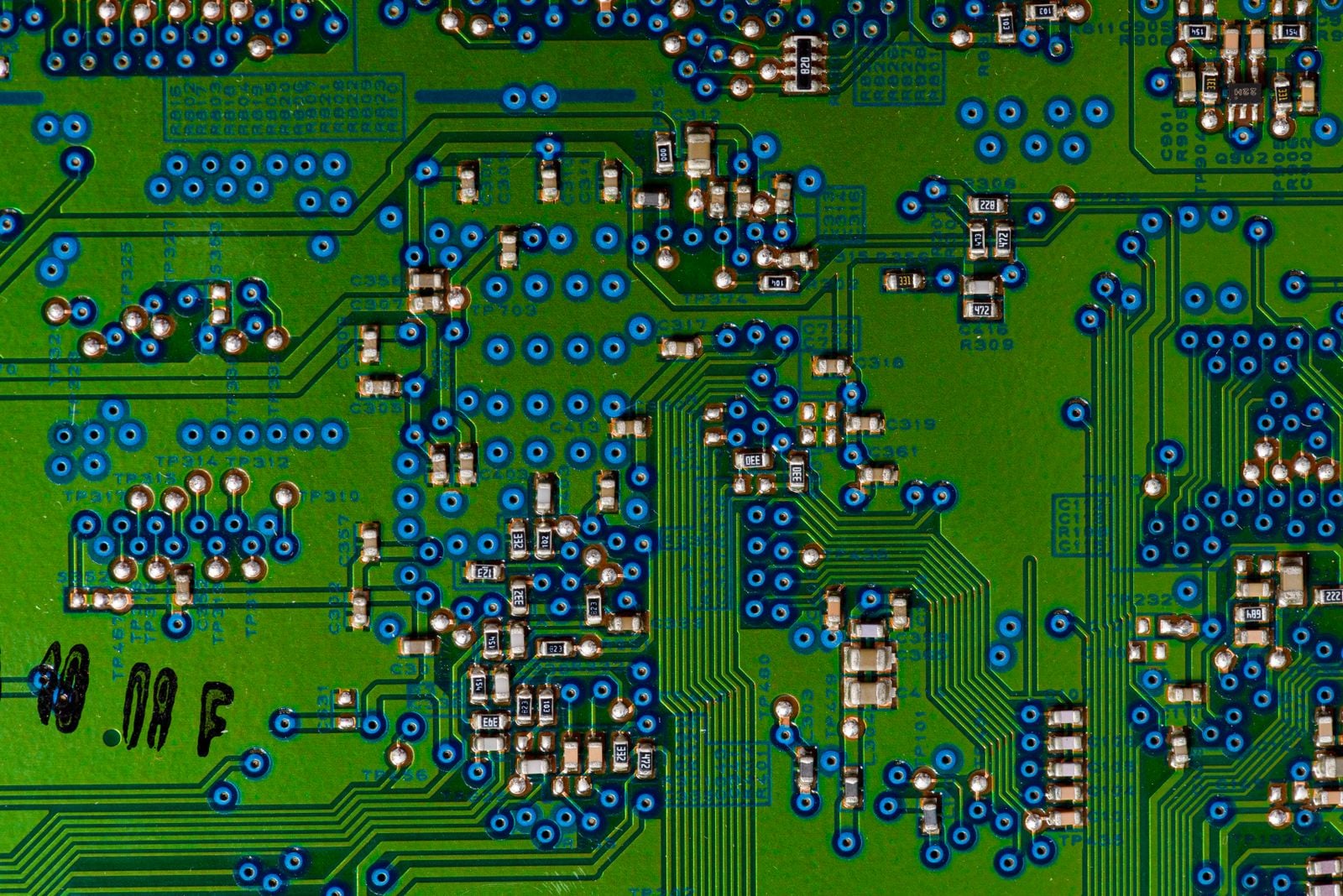
Somewhere inside the phone in a pocket, a switch is flipping on and off about five billion times a second. There are tens of billions of these switches packed onto a chip the size of a fingernail, and the smallest features on the newest ones measure around three nanometres — a distance so short that laying silicon atoms end to end, you’d fit only about fifteen of them across. That isn’t a marketing figure so much as a warning sign. The transistor, the tiny electrical valve that every computer is built from, is running out of room to shrink.
The transistor was invented at Bell Labs in December 1947, when John Bardeen and Walter Brattain pressed two gold contacts into a sliver of germanium and watched a small current control a much larger one. That first device was roughly a centimetre across. The 1956 Nobel Prize in Physics went to Bardeen, Brattain and William Shockley for the discovery. Everything since — every laptop, every satellite, every pacemaker — is a story of making that same switch smaller, faster and more numerous.
What “3 nanometres” actually means
The number is slippery. When Intel, TSMC or Samsung advertise a “3 nm” or “2 nm” process, they are not saying any single feature on the chip measures exactly that. Since roughly the 22 nm generation, the node name has been a marketing label rather than a physical dimension. The IEEE International Roadmap for Devices and Systems tracks the real numbers, and they are still astonishingly small: gate lengths on the newest logic transistors are in the range of 12 to 16 nanometres, and some critical dielectric layers are only a handful of atoms thick.
A silicon atom has a diameter of about 0.2 nanometres. So a 3 nm feature really is on the order of 15 atoms across, and a 1 nm-thick gate oxide is roughly four or five atoms of insulation between the switching electrode and the channel where current flows. At that scale, the chip has stopped being a landscape you sculpt and started being something closer to chemistry — a lattice where every atom counts.
Why smaller was always the point
In 1965, Gordon Moore, then at Fairchild Semiconductor, wrote a short trade-magazine article predicting that the number of components on an integrated circuit would roughly double every year. He later revised it to every two years. The industry took the prediction as a target, and for half a century it hit it. Intel’s own history of Moore’s Law notes that a 1971 Intel 4004 held 2,300 transistors. A modern high-end processor holds more than 100 billion.
Shrinking helps in three ways at once. Smaller transistors switch faster, because electrons cover less distance. They use less energy per switch, because there is less capacitance to charge. And more of them fit in the same area, so a single chip can do more work. The virtuous loop is why a phone today outperforms the supercomputers of the 1990s while running on a battery.
What starts going wrong at this scale
The trouble is that “small” eventually stops being an engineering problem and becomes a physics problem. At a few nanometres, electrons no longer behave like reliable little balls of charge. They start to tunnel — a quantum-mechanical effect in which a particle appears on the far side of a barrier it doesn’t have the energy to cross. In a transistor, that means current leaks through the gate insulator even when the switch is nominally off. The thinner the insulator, the worse it gets. Leakage current, heat and device-to-device variability now dominate the design of leading-edge nodes, and each new generation buys less headroom than the last.
There is also the problem of counting atoms. When a transistor channel is only a few dozen atoms wide, whether a particular dopant atom ends up on the left or the right of the channel changes the device’s behaviour measurably. Billions of transistors on a chip means billions of slightly different transistors, and the circuit has to work anyway. Manufacturers compensate with error correction, redundancy and clever architecture, but the raw material is getting harder to tame.
The switch from FinFET to gate-all-around
To keep going, chipmakers have changed the shape of the transistor itself. For roughly a decade the industry used a design called FinFET, in which the current-carrying channel stands up like a shark fin so the gate can wrap around it on three sides and keep better control of the electrons. At 3 nm and below, even that isn’t enough. Samsung’s 3 nm process, introduced in 2022, and TSMC’s and Intel’s next generations use a structure called gate-all-around, or nanosheet, transistors, where the channel is a stack of horizontal ribbons completely surrounded by the gate on all four sides. The geometry buys a few more shrinks. It does not repeal quantum mechanics.
Fabricating features this small also requires light with a wavelength smaller than the features themselves. That is why the industry has moved to extreme ultraviolet lithography at 13.5 nanometres, generated by vaporising tin droplets with a laser 50,000 times a second inside a vacuum chamber. Each EUV machine, built almost exclusively by the Dutch company ASML, costs on the order of 200 million dollars and weighs about 180 tonnes. A single leading-edge fab can hold dozens of them.
How close is the wall?
Estimates vary, but most physicists agree that a silicon transistor cannot usefully be shrunk below about 1 nanometre for the gate length — roughly five atoms across. Below that, tunnelling makes the switch effectively always-on. In 2022, researchers at Tsinghua University reported a transistor with a gate length of 0.34 nm, the thickness of a single graphene sheet, published in Nature. It is a laboratory curiosity, not a manufacturing process, but it hints at how the endgame might look: exotic two-dimensional materials replacing silicon entirely.
The industry’s near-term plan is less dramatic. Rather than shrinking the transistor much further, chipmakers are stacking them — building 3D chips where logic sits on top of memory sits on top of more logic, connected by vertical vias only a few micrometres wide. This is why nodes named “2 nm” and “18 Å” (angstroms — 0.1 nm each) are still on the roadmap even though nothing on the chip is really that small. The label refers to the density and performance a generation delivers, not to any measurable feature.
What “the limit” really means
The end of transistor shrinking is not the end of computing. It is the end of a very specific bargain — the one that let each generation of chips be faster and cheaper than the last, almost automatically, for fifty years. From here on, the gains come from architecture: specialised accelerators for AI and graphics, better memory hierarchies, chiplets glued together in a single package, and eventually perhaps optical or superconducting logic. The transistor, in some form, will probably still be there. It just won’t be getting much smaller.
Every time a phone unlocks with a face, a few hundred billion of these atom-scale switches flip in concert to decide the answer. They are among the smallest working machines humans have ever built, and they are almost as small as physics is going to allow.