

The size of a processor’s process node is always something that’s frequently discussed in the chip’s specifications. But what is that, and why does it matter?
What does “process size” mean?
In this context, “process” is used to describe the fabrication process rather than the computer’s processor. It’s about how the chip gets made, not what it can do. The size of the process node, measured in nanometers, describes the size of a processor’s smallest possible element.
Imagine it like this: If a processor’s design is a digital image, the size of one “pixel” would be the process size. For example, on Intel’s current process, the smallest possible element is 14 nanometers, or 14nm. The smaller the process, the greater the resolution that can be obtained. As a result, fabricators can make transistors and other components smaller. This means that more transistors can be crammed into a smaller physical space. This provides some major benefits as well as a couple downsides.
Why is smaller better?

If you shrink all parts of a transistor equally, the electrical properties of that transistor will not change. And the more transistors you can fit in a given space, the greater processing power you’ll have. This is thanks to increases in computational parallelism and cache sizes. So if you’re trying to speed up a chip or add new features, there’s a strong incentive to shrink the size of its transistors.
Smaller processes also have a lower capacitance, allowing transistors to turn on and off more quickly while using less energy. And if you’re trying to make a better chip, that’s perfect. The faster a transistor can toggle on and off, the faster it can do work. And transistors that turn on and off with less energy are more efficient, reducing the operating power, or “dynamic power consumption,” required by a processor. A chip with lower dynamic power consumption will drain batteries more slowly, cost less to run, and be more ecologically friendly.
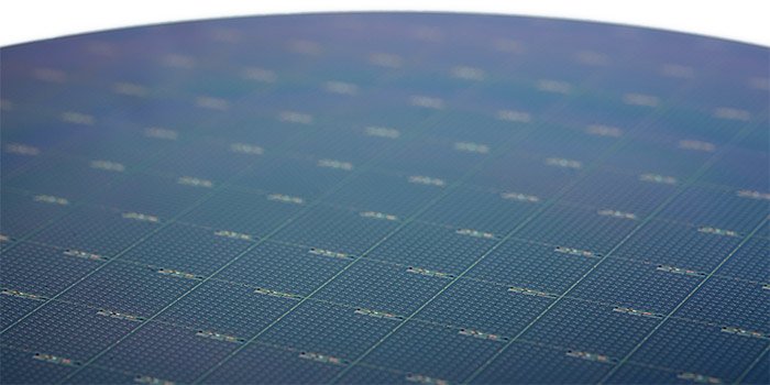
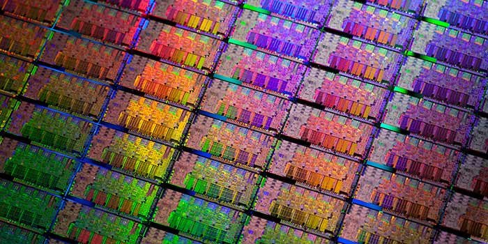
Smaller chips are also less expensive to make. Chips are made on circular wafers of silicon, like the one above. A single wafer will typically contain dozens of processor dies. A smaller process size will create a smaller die size. And if die size is smaller, more dies will fit on a single silicon wafer. This leads to an increase in manufacturing efficiency, reducing fabrication costs. Developing a new process does require major investment, but after that cost is recovered, per-die costs drop significantly.
Also read: What Is Microsoft’s Pluton Security Processor and Why You Need It
What is the downside of a smaller process size?
Smaller transistors are harder to make. As transistors shrink, it becomes harder and harder to make chips that run at the highest possible clock speed. Some chips won’t be able to run at top speed, and these chips will get “binned,” or labelled, as chips with lower clock speeds or smaller caches. Smaller processes generally have more chips binned at lower clock speeds since making a “perfect” chip is more challenging. Fabricators are careful to eliminate as many issues as possible, but it often comes down to the unavoidable variations of the analog world.
Smaller transistors also have greater “leakage.” Leakage is a measurement of how much current a transistor allows through when in the “off” position. This means that as leakage increases, so does the static power consumption or the amount of power a transistor consumes while idle. A chip with greater leakage requires more power even when it’s not active, draining batteries faster and running less efficiently.
A smaller process might have a lower yield, resulting in fewer fully functional chips. This can cause production delays and shortages. That makes it harder to recoup the investment required to develop a new process. This element of risk underlies any new manufacturing process, but its especially true for a process as precise as semiconductor fabrication.
Of course, manufacturers attempt to reduce or eliminate these problems when developing a new process, and they’re frequently successful. That’s why we get chips that are faster and more efficient even as process size shrinks.
Conclusion
Shrinking process size is difficult, but the benefits create a strong incentive for manufacturers to chase smaller and smaller process sizes. And thanks to that drive, consumers get faster, more efficient chips every couple of years. It’s these advances that made technological marvels like smartphones possible, and that will enable the next generation of technological achievements.